1 1.江苏大学 材料科学与工程学院, 镇江212013
2 2.中国科学院 上海硅酸盐研究所, 透明光功能无机材料重点实验室, 上海 201899
3 3.华北光电技术研究所 固体激光科学与技术实验室, 北京100015
4 4.中国科学院大学 材料与光电研究中心, 北京 100049
Yb:YAG透明陶瓷由于具有宽的吸收带和发射带、高增益、低的热负载、长的荧光寿命、高的量子效率等优点而成为有应用前景的高功率固体激光器用增益介质。本研究优化了粉体的性能并制备了高透明的Yb:YAG陶瓷。以碳酸氢铵为沉淀剂, 分别以纯水或乙醇/水混合物为溶剂, 采用共沉淀法合成了5at%Yb:YAG纳米粉体。在1250 ℃下煅烧4 h得到的所有粉体均为纯YAG相。与纯水溶剂制备的粉体相比, 醇水溶剂制备的粉体具有更小的平均晶粒尺寸和更低的团聚程度。以醇水溶剂制备的粉体为原料, 采用真空烧结法在不添加烧结助剂的情况下成功制备了5at%Yb:YAG透明陶瓷, 并对1500~1825 ℃烧结20 h和1800 ℃烧结10~50 h所得陶瓷的微观结构和直线透过率进行了探究。除在1825 ℃下烧结20 h所得的陶瓷外, 其余的5at%Yb:YAG陶瓷都具有均匀的微观结构。在1800 ℃下烧结50 h制备的5at%Yb:YAG陶瓷具有最高的光学质量, 在1100和400 nm处的直线透过率分别为78.6%和76.7%(样品厚度为2.2 mm)。该Yb:YAG透明陶瓷在937 nm处的吸收截面为5.03×10⁻²¹ cm2, 在1031 nm处的发射截面为13.48×10⁻²¹cm2。
Yb:YAG透明陶瓷 醇水共沉淀法 真空烧结 微观结构 光学性能 Yb:YAG transparent ceramic alcohol-water co-precipitation vacuum sintering microstructure optical property 
Author Affiliations
Abstract
1 State Key Laboratory of Information Photonics and Optical Communications, Beijing University of Posts and Telecommunications, Beijing 100876, China
2 Guangxi Key Laboratory of Wireless Wideband Communication and Signal Processing, Guilin 541004, China
3 College of Optical Sciences, The University of Arizona, Tucson, Arizona 85721, USA
4 e-mail: dabombyh@aliyun.com
Metasurfaces have pioneered a new avenue for advanced wave-front engineering. Among the various types of metasurfaces, Huygens’ metasurfaces are thought to be a novel paradigm for flat optical devices. Enabled by spectrally overlapped electric resonance and magnetic resonance, Huygens’ metasurfaces are imparted with high transmission and full phase coverage of , which makes them capable of realizing high-efficiency wave-front control. However, a defect of Huygens’ metasurfaces is that their phase profiles and transmissive responses are often sensitive to the interaction of neighboring Huygens’ elements. Consequently, the original assigned phase distribution can be distorted. In this work, we present our design strategy of transmissive Huygens’ metasurfaces performing anomalous refraction. We illustrate the investigation of Huygens’ elements, realizing the overlapping between an electric dipole and magnetic dipole resonance based on cross-shaped structures. We find that the traditional discrete equidistant-phase design method is not enough to realize a transmissive Huygens’ surface due to the interaction between neighboring Huygens’ elements. Therefore, we introduce an extra optimization process on the element spacing to palliate the phase distortion resulting from the element interaction. Based on this method, we successfully design unequally spaced three-element transmissive metasurfaces exhibiting anomalous refraction effect. The anomalous refractive angle of the designed Huygens’ metasurface is 30°, which exceeds the angles of most present transmissive Huygens’ metasurfaces. A transmissive efficiency of 83.5% is numerically derived at the operating wavelength. The far-field electric distribution shows that about 93% of transmissive light is directed along the 30° refractive direction. The deflection angle can be tuned by adjusting the number of Huygens’ elements in one metasurface unit cell. The design strategies used in this paper can be inspiring for other functional Huygens’ metasurface schemes.
Photonics Research
2019, 7(12): 12001501
Author Affiliations
Abstract
1 State Key Laboratory of Information Photonics and Optical Communications, Beijing University of Posts and Telecommunications, Beijing 100876, China
2 School of Science, Beijing University of Posts and Telecommunications, Beijing 100876, China
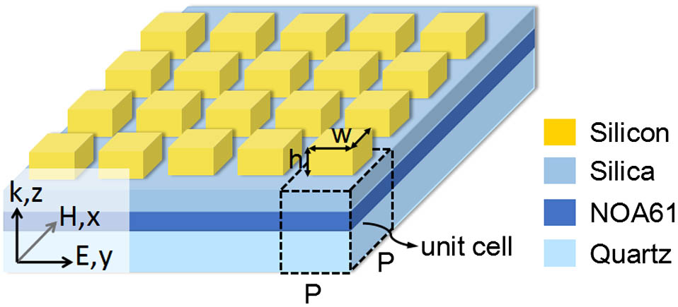
We propose and numerically investigate an efficient transmission-mode metasurface that consists of quasi-continuous trapezoid-shaped crystalline silicon nanoantennas on a quartz substrate. This metasurface provides a linear phase gradient and realizes both full 2π phase shift and high transmission efficiency in the operating wavelength range from 740 to 780 nm. At the central wavelength around 751 nm, the total transmission efficiency is up to 88.0% and the section of the desired anomalous refraction is 80.4%. The anomalous refraction angle is 29.62°, and larger refraction angle can be achieved by changing the period of the super cell. We demonstrate a refraction angle as large as 38.59°, and the anomalous transmission efficiency reaches 76.6% at wavelength of 741 nm. It is worth mentioning that the structure is much simpler than conventional metasurfaces based on arrays of discrete nanoantennas. Our research may pave the way for designing efficient all-dielectric phase-gradient metasurfaces and applying them in integrated optical devices for wavefront control.
Metamaterials Phase shift Integrated optics devices Photonics Research
2018, 6(6): 06000517

Author Affiliations
Abstract
State Key Laboratory of Information Photonics and Optical Communications, Beijing University of Posts and Telecommunications, Beijing 100876, China
A novel scheme for the design of an ultra-compact and high-performance optical switch is proposed and investigated numerically. Based on a standard silicon (Si) photonic stripe waveguide, a section of hyperbolic metamaterials (HMM) consisting of 20-pair alternating vanadium dioxide (VO2)/Si thin layers is inserted to realize the switching of fundamental TE mode propagation. Finite-element-method simulation results show that, with the help of an HMM with a size of 400 nm×220 nm×200 nm (width×height×length), the ON/OFF switching for fundamental TE mode propagation in an Si waveguide can be characterized by modulation depth (MD) of 5.6 dB and insertion loss (IL) of 1.25 dB. It also allows for a relatively wide operating bandwidth of 215 nm maintaining MD>5 dB and IL<1.25 dB. Furthermore, we discuss that the tungsten-doped VO2 layers could be useful for reducing metal-insulator-transition temperature and thus improving switching performance. In general, our findings may provide some useful ideas for optical switch design and application in an on-chip all-optical communication system with a demanding integration level.
Optical switching devices Integrated optics devices Metamaterials Photonics Research
2017, 5(4): 04000335
Author Affiliations
Abstract
State Key Laboratory of Information Photonics and Optical Communications, Beijing University of Posts and Telecommunications, Beijing 100876, China
We propose new types of hybrid plasmonic waveguides for low-threshold nanolaser applications. Modal properties and lasing threshold under different geometric shapes and parameters are investigated and -analyzed by the finite element method, aiming to realize both low propagation and high field confinement. Results show that a smaller gap width and a larger round corner radius of the metal film reduce the lasing threshold. These new structures can open up new avenues in the fields of active plasmonic circuits.
240.6680 Surface plasmons 140.5960 Semiconductor lasers 350.5500 Propagation Chinese Optics Letters
2014, 12(11): 112401
Author Affiliations
Abstract
State Key Laboratory of Information Photonics and Optical Communications, Beijing University of Posts and Telecommunications, Beijing 100876, China
We propose and analyze a long-range dielectric-loaded surface plasmon polariton (SPP) waveguide based on graded-index ridge over server millimeter distances. Then the influence of the dielectric thickness and the ridge refractive index on propagation length and mode width is discussed and simulated with the finite ele-ment method. The result shows that the SPP can propagate as long as 3.42 mm, as well as the mode width keeping as 1.64 mm, a better one compared with the fixed refractive index. Considering its nanoscale dimen-sion and outstanding performance, the structure is easily realized when connected with electrodes.
240.6680 Surface plasmons 160.4236 Nanomaterials 230.7370 Waveguides Chinese Optics Letters
2014, 12(9): 092402
Author Affiliations
Abstract
A nonlinear hybrid plasmonic slot waveguide composed of periodically poled lithium niobate (PPLN) and two separated silver films is investigated. The effective refractive index, propagation length, and energy confinement of the hybrid anti-symmetric mode in this waveguide are calculated using the structure parameters at the fundamental wavelength of \lambda=1550 nm and its second harmonic (SH) \lambda= 775 nm. Through the above indices, coupling efficiency (maximum SH conversion efficiency during propagation) and peak position (propagation location of the conversion efficiency) of SH generation are analyzed. Finally, higher conversion efficiency can be achieved at a shorter propagation distance by changing the waveguide into a tapered structure.
190.2620 Harmonic generation and mixing 240.6680 Surface plasmons 230.7370 Waveguides Chinese Optics Letters
2013, 11(10): 101901
北京邮电大学信息光子学与光通信国家重点实验室, 北京 100876
从矩形空气孔光子晶体平板的研究入手,设计了一种新型的正方形空气孔L3型光子晶体平板微腔。采用有限时域差分法,计算了正方形空气孔L3型光子晶体微腔的Q值、模体积及谐振频率;讨论了正方形空气孔边长对微腔Q值、模体积及谐振频率的影响。对L3型光子晶体平板微腔进行了优化,设计出了Q值为27719、模体积为0.4361(λ/n)3、谐振波长为1543 nm的正方形空气孔的L3型光子晶体平板微腔。该L3型光子晶体平板微腔的Purcell因子高达4767。
材料 光电子学 光子晶体微腔 Q值 模体积 Purcell因子 光学学报
2013, 33(11): 1116005
北京邮电大学信息光子学与光通信国家重点实验室, 北京 100876
采用有限元法,计算了二维三角晶格椭圆形格点空气孔型光子晶体的TE、TM模式的带隙结构。通过对椭圆形空气孔格点的大小、方向进行改变,研究了填充比、格点方向对带隙的影响。计算结果表明,在空气孔型光子晶体中TE模式更容易形成带隙;不同填充比情况下,格点方向对TE模式和TM模的带隙变化都具有不同影响;不论格点方向如何变化,均未出现完全带隙。
非线性光学 光子晶体 光子带隙 有限元法 完全光子带隙


